38 phase locked loop block diagram
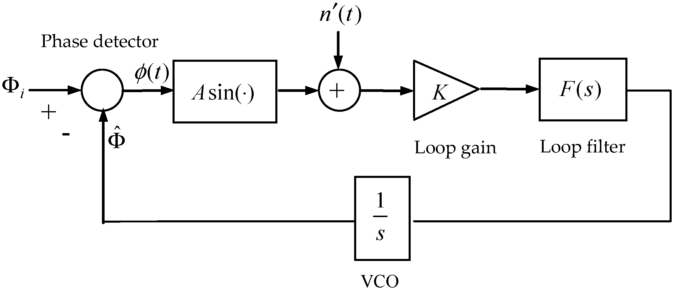
PDF Phase Locked Loops Design And Analysis Phase-locked loops (PLL) Nonlinear design and analysis. Introduction. Block diagram and mathematical model of PLL. Figure 4: Block diagram of PLL on the level of phase relations. Consider now the high-frequency oscillators, connected by a diagram in Fig. Demo: Phase Locked Loop A phase-locked loop (PLL) is a closed-loop feedback control system that generates and outputs a signal in relation to the frequency and phase of an Since an integrated circuit can hold a complete phase-locked loop building block, the technique is widely used in modern electronic devices, with...
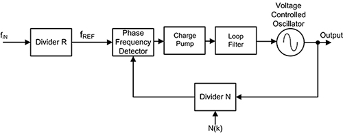
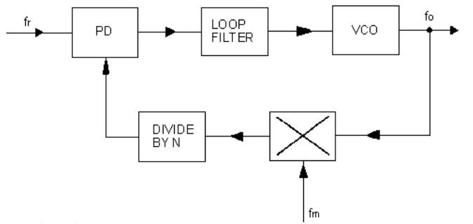
PLL Working | Phase Locked Loop Working operation The figure-1 depicts Block Diagram of Phase locked loop i.e. PLL Circuit in order to explain PLL working operation. PLL mathematical equation can be expressed as Fo = Fr * N , Hence Fo can be changed to different values within the range in either of the following ways.

Phase locked loop block diagram
Phase Locked Loop (PLL) and Delay Locked Loop... - Open4Tech 1 PLL block diagram. The basic operation of PLL can be divided into 3 steps. Delay-Locked Loop (DLL). The DLL is used for phase syncronisation of a reference clock with a system clock. Both the reference clock (CLK_IN) and the system clock (CLK_OUT) have the same frequency. Phase Locked Loops - an overview | ScienceDirect Topics Phase-locked loops (PLLs) have many applications in the communications world. The main purpose of a PLL circuit is to synchronize an output oscillator Block diagram of a PLL. We can readily model a PLL at this level in VHDL-AMS. We implement the phase detector as an analog multiplier, the loop... Phase Locked Loops (PLL) and Frequency Synthesis Phase Locked Loops (PLL) are ubiquitous circuits used in countless communication and engineering applications. A PLL is a truly mixed-signal circuit, involving the co-design of RF, digital, and analog building blocks. A non-linear negative feedback loop that locks the phase of a VCO to a reference...
Phase locked loop block diagram. PDF Oscillation Control in CMOS Phase-Locked Loops 1 A general PLL block diagram 2 Phase-locked loop 3 Block diagram of the linear PLL 4 Characteristic of an analog mixer 5 XOR phase detector behavior 6 Characteristic of an XOR The most fundamental block diagram of a PLL is shown in Figure 1 [1]. A PLL differs from other feedback... Flip-flop (electronics) - Wikipedia In electronics, a flip-flop or latch is a circuit that has two stable states and can be used to store state information – a bistable multivibrator.The circuit can be made to change state by signals applied to one or more control inputs and will have one or two outputs. PLL Phase Locked Loop: How it Works » Electronics Notes The phase locked loop or PLL is a particularly useful circuit block that is widely used in radio frequency or wireless applications. In view of its usefulness, the phase locked loop or PLL is found in many wireless, radio, and general electronic items from mobile phones to broadcast radios... PDF Fpga-based digital phase-locked loop analysis and Phase-locked loop (PLL) is a linear feedback control system that can gener-ate an output signal which has the same frequency and, perhaps, phase as the input Figure 1 (gures are grouped at the end of each chapter) shows the generic block diagram for digital PLL. We denote input signal as x[n] = cos...
Phase Locked Loop Integrated Circuit Phase locked loops (PLLs) can be found in many different types of circuits nowadays. Their applications range from a variety of uses. Figure 25: Simple Ring Oscillator Circuit Block Diagram At every run through the system, each node oscillates between a 1 and 0 due to the inverting action. PDF Practical Phase-Locked Loop | Charge-Pump PLL Building Blocks Practical Phase-Locked Loop Design. 2004 ISSCC Tutorial Dennis Fischette. • A PLL is a negative feedback system where an oscillator-generated signal is phase and frequency locked to a reference signal. Charge-Pump PLL Block Diagram. PDF Tutorial on Digital Phase-Locked Loops Why Are Digital Phase-Locked Loops Interesting? Just Enough PLL Background … What is a Phase-Locked Loop (PLL)? ƒ The standard analog PLL implementation is. problematic in many applications. - Analog building blocks on a mostly digital chip pose design and verification challenges. PDF Phase-Locked Loop Design Fundamentals Phase-Locked Loop Design Fundamentals. by: Garth Nash Applications Engineering. Abstract. The design of a PLL typically involves determining the type of loop required, selecting the proper Laplace Representation of diagram in Figure 11. Phase-Locked Loop Design Fundamentals Application...
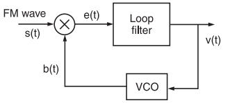
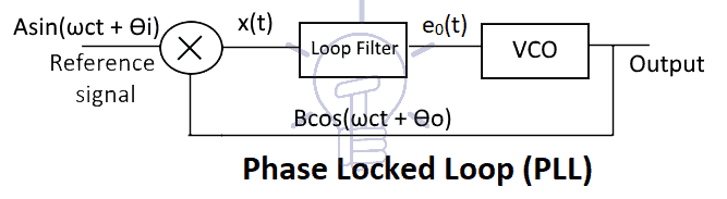
PDF PFD-CP Phase Locked Loop | Chapter 2. PLL function blocks design phase-locked is called the lock-in range or capture range. For a PLL using PFD and charge pump, the hold range is also only limited by the VCO output frequency range. Every building block of the PLL will contribute to the total output noise. The noise sources of the PLL are shown in the following figure. Writing a Phase-locked Loop in Straight C - liquidsdr.org As its name implies, a phase-locked loop (PLL) is designed to lock the phase of an oscillator to the phase of a reference signal, providing a mechanism for synchronization on different platforms. [analog_pll_diagram] depicts a simplified continuous-time analog PLL. SAM D21/DA1 Family - Microchip Technology – Internal and external clock options with 48 MHz Digital Frequency-Locked Loop (DFLL48M) and 48 MHz to 96 MHz Fractional Digital Phase-Locked Loop (FDPLL96M) – External Interrupt Controller (EIC) – 16 external interrupts – One Non-maskable Interrupt (NMI) – Two-pin Serial Wire Debug (SWD) programming, test and debugging interface ... Single Phase Full Bridge Inverter | DC-TO-AC INVERTER ... A single phase bridge DC-AC inverter is shown in Figure below. The analysis of the single phase DC-AC inverters is done taking into account following assumptions and conventions. 1) The current entering node a in Figure 8 is considered to be positive. 2) The switches S1, S2, S3 and S4 are unidirectional, i.e. they conduct current in one direction.
Demystifying phase-locked loops - Embedded.com
Phase-locked loop - Wikipedia A phase-locked loop or phase lock loop (PLL) is a control system that generates an output signal whose phase is related to the phase of an input signal.
Clock Generation Using PLL Frequency Synthesizers | DigiKey
PDF Synthesis of Phase-Locked Loop: analytical methods and simulation Phase-locked loop (PLL) is a circuit invented by a French engineer Anri de Belles-cize in the 1930s (Bellescize, 1932). One of the rst applications of PLL was in the wireless communication (Wendt and Fredentall, 1943; Richman, 1954). In radio-engineering, PLL-based circuits (e.g., a PLL system with a...
Glossary Definition for Phase-Locked Loop
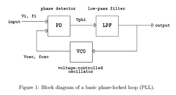
Digital Phase Locked Loop Phase Locked Loops are used in almost every communication system. Some of its uses include The below figure(1-1) shows the basic block diagram of PLL which consists of PFD , loop filter and VCO. Phase Locked Loops (PLLs) are widely used for frequency synthesis in many Applications...

General block diagram of ADPLL Beginning of all digital phase ...
RF Agile Transceiver Data Sheet AD9361 - Analog Devices The fully integrated phase-locked loops (PLLs) provide low power fractional-N frequency synthesis for all receive and transmit channels. Channel isolation, demanded by frequency division duplex (FDD) systems, is integrated into the design. All VCO and loop filter components are integrated. The core of the AD9361 can be powered directly from a 1.3 V
PLL FM Demodulator (Phase Locked Loop FM Demodulator ...
Three Phase Inverter | DC-TO-AC INVERTER || Electronics Tutorial As in a single-phase square-wave inverter, switches in each leg of the three-phase inverter operate in a complementary manner. When upper switch of a leg is on the lower switch will need to block the entire dc bus voltage and vice versa. Thus the switches must be rated to block the worst-case instantaneous magnitude of dc bus voltage.

Phase Lock Loop - abisceg
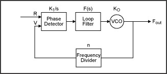
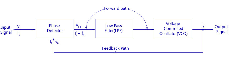
PDF Phase locked loop | Basic Block Diagram of a PLL Forward path When Phase locked, the loop tracks any change in the input frequency through its repetitive action. If an input signal vs of frequency fs is applied to the PLL, the phase detector compares the phase and frequency of the incoming signal to that of the output vo of the VCO.

Driving the VCO of a High Voltage Phase-Locked Loop Frequency ...
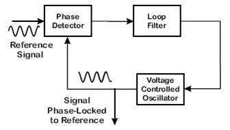
Understanding Phase-Locked Loops Figure 2: Phase-locked loop block diagram. In the weatherfax project, one of the key design issues was to convert a range of audio tones into a video At its most basic, a phase-locked loop (hereafter PLL) compares the frequency of a local reference oscillator to that of a received signal, and uses a...

Phase Locked Loop Project Overview for Analog Integrated ...
Phase Locked Loops, block diagram, working, operation, Design... The block diagram consist of a phase detector which acts as a phase comparator, an amplifier, and a low pass filter with the combination of the resistor The lock range usually increases with an increase in input voltage but falls with an increase in supply voltage. Phase Locked Loop (PLL) - Working.

Block Diagram of a Phase Locked Loop (Courtesy:... | Download ...
PDF 2.1. Basic operation of a Phase-Locked Loop (PLL) PHASE-LOCKED AND DELAY-LOCKED LOOPS A Dissertation. Presented in Partial Fulfillment of the Requirements for the Degree of Doctor of Philosophy with a Major in Electrical Engineering in the College of Graduate Studies University of Idaho. by Feng Lin.
Phase Locked Loop (PLL) - its Operation, Characteristics ...
PDF CMOS Phase-Locked-Loop Applications (Rev. B) CMOS Phase-Locked-Loop Applications Using the CD54/74HC/HCT4046A and CD54/74HC/HCT7046A. W. M. Austin. Standard Linear & Logic. ABSTRACT. Applications of the HC/HCT4046A phase-locked loop (PLL) and HC/HCT7046A PLL with lock detection are provided...

Phase-Locked Loop (PLL) Fundamentals | Analog Devices
PDF Introduction to Phase Locked Loop (PLL) Phase Locked Loop (PLL) is a fundamental part of radio, wireless and telecommunication technology. The goal of this document is to review the theory, design and analysis of PLL circuits. A block diagram of a programmable divider using a dual modulus divider is shown in Figure 9.
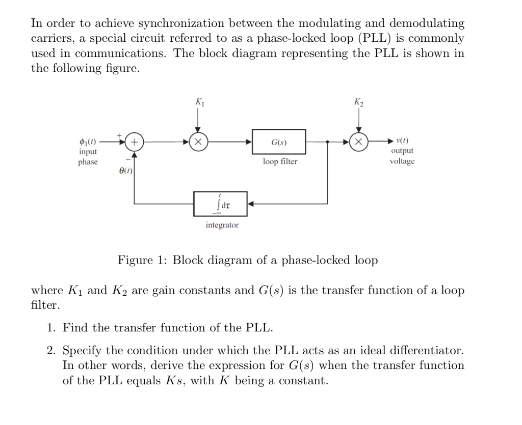
Solved In order to achieve synchronization between the ...
Phase locked loop block diagram - YouTube Phase Lock Loop basics, Block Diagram & working in Communication Engineering by Engineering Funda. phase locked loop (PLL) with block diagram explained in Telugu. #phaselockedloop #PLL.
Phase Locked Loop Operating Principle and Applications
Phase-locked loop A phase locked loop or phase lock loop (PLL) is a control system that generates an output signal whose phase is related to the 4.7 Frequency Synthesis. 5 Phase-locked loop block diagram. 6 Elements. Phase-locked loop mechanisms may be implemented as either analog or digital circuits.
Lab_6,7,8) Phase Lock Loop - D.Son978
PDF Xilinx XAPP854 Digital Phase-Locked Loop (DPLL) Reference Design... Application Note: Virtex-4 FPGAs. Digital Phase-Locked Loop (DPLL) Reference Design. Figure 1 is a block diagram of the DPLL reference design. In addition to the Virtex-4 FPGA, the design requires two external components: a low-cost digital-to-analog converter (DAC) and a voltage-controlled...
What is Phase Lock Loop (PLL)? How Phase Lock Loop Works ? PLL Explained
Phase-Locked Loop (PLL) Fundamentals | Analog Devices Phase-locked loop (PLL) circuits exist in a wide variety of high frequency applications, from simple clock clean-up circuits, to local oscillators (LOs) for This article explains some of the building blocks of phase locked loop circuits with references to each of these applications, in turn, to help guide the...

Phase-locked loop control system | Download Scientific Diagram
Phase Locked Loop Operating Principle and Applications The below figure shows the block diagram of the PLL. Phase-Locked Loop Detector. The phase-locked loop detector compares the input frequency and the output frequency of the VCO to produces a DC voltage which is directly proportional to the phase distinction of the two frequencies.

Demo: Phase Locked Loop
PDF Phase-Locked Loop Basics (PLL) | Charge-Pump PLL Block Diagram Charge-Pump PLL Block Diagram. RefClk Phase-Freq. Detector. [1] B. Razavi, Monolithic Phase-Locked Loops and Clock-Recovery Circuits, IEEE Press, 1996. - collection of IEEE PLL papers. [2] I. Young et al., "A PLL clock generator with 5 to 110 MHz of lock range for...

Dual Phase-Locked Loop Option | Zurich Instruments
Phase Locked Loops (PLL) and Frequency Synthesis Phase Locked Loops (PLL) are ubiquitous circuits used in countless communication and engineering applications. A PLL is a truly mixed-signal circuit, involving the co-design of RF, digital, and analog building blocks. A non-linear negative feedback loop that locks the phase of a VCO to a reference...

Phase-Locked Loop Design and Construction - Elliot Nwaobi ...
Phase Locked Loops - an overview | ScienceDirect Topics Phase-locked loops (PLLs) have many applications in the communications world. The main purpose of a PLL circuit is to synchronize an output oscillator Block diagram of a PLL. We can readily model a PLL at this level in VHDL-AMS. We implement the phase detector as an analog multiplier, the loop...

Simulation block diagram for a classical digital phase locked ...
Phase Locked Loop (PLL) and Delay Locked Loop... - Open4Tech 1 PLL block diagram. The basic operation of PLL can be divided into 3 steps. Delay-Locked Loop (DLL). The DLL is used for phase syncronisation of a reference clock with a system clock. Both the reference clock (CLK_IN) and the system clock (CLK_OUT) have the same frequency.

Describe the basic block diagram of the phase locked loop (PLL).
VCO15-10 - Phase locked loop fundamentals

Block diagram of Phase-Locked Loop (PLL). | Download ...

Demo: Phase Locked Loop
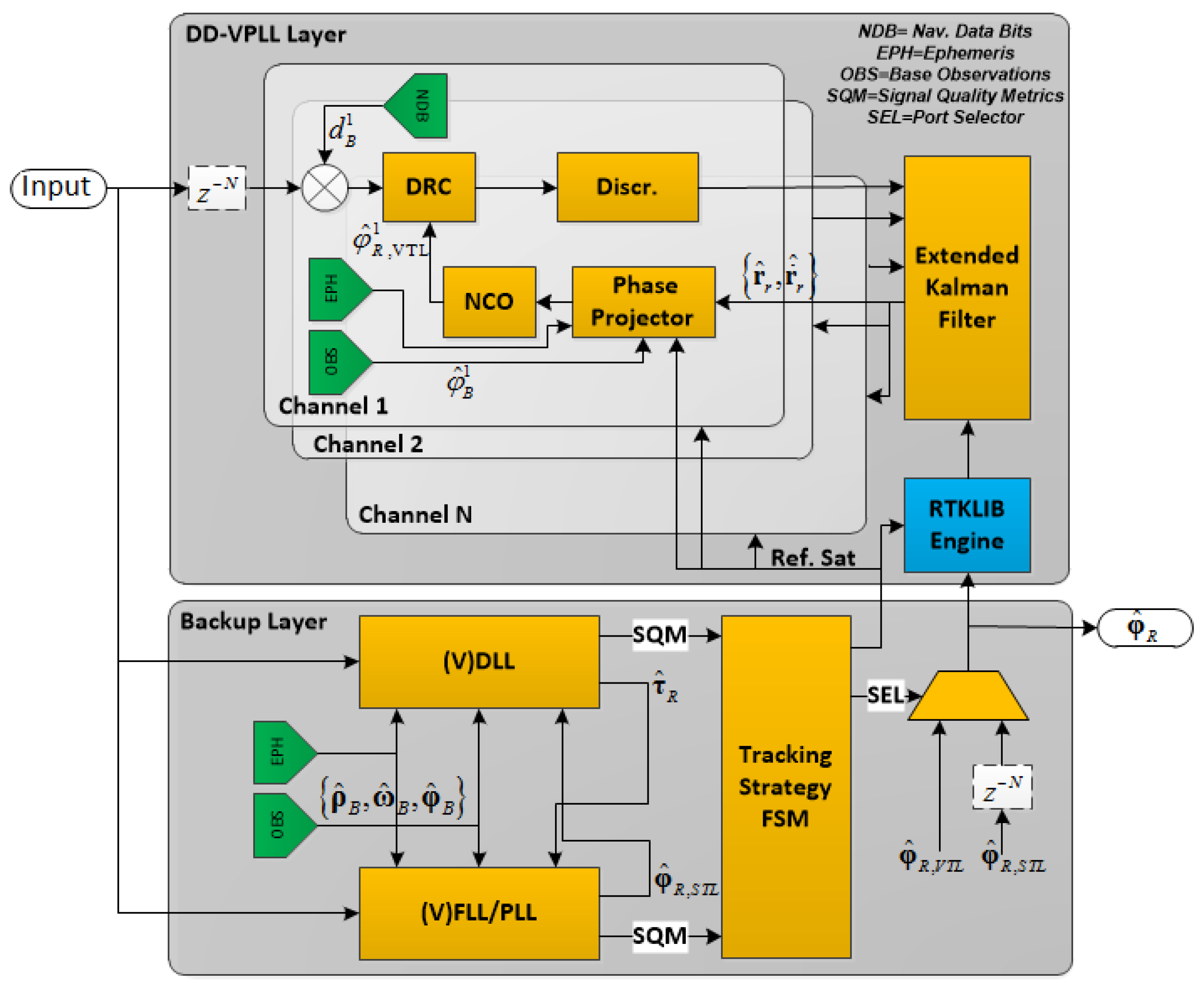
Sensors | Free Full-Text | Design and Implementation of an ...
Is it possible to analyze the operation of PLL (phase locked ...

Simulation block diagram for a classical digital phase locked ...
Applied Sciences | Free Full-Text | Investigation of Phase ...

PLL DesignGuide Reference - ADS 2008 Update 1 - Keysight ...

1: Block diagram of a Phase-Locked Loop. | Download ...
Optical Phase Locking techniques: an overview and a novel ...
PHASE LOCKED LOOP
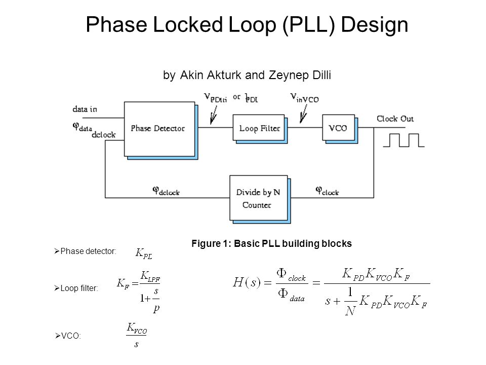
Phase detector: Loop filter: VCO: Phase Locked Loop ...
Integrated electro-optical phase-locked loop for high ...

Electronics | Free Full-Text | A Design of Wide-Range and Low ...

PLL Tab :: Zurich Instruments Documentation
Phase-Locked-Loop | Mini Projects | Electronics tutorial ...

Phase Locked Loop (PLL) and Delay Locked Loop (DLL) Basics ...
0 Response to "38 phase locked loop block diagram"
Post a Comment